NHD-C0220Biz-FS(RGB)-FBW-3VM Pins backwards on manufacture document?

-

Hello,
I have used this display and the pinouts do confuse a few people.
However i can confirm that when you are looking at the front of the display the pin on the far right is the Reset pin.
The schematic on EasyEDA might be looking at the display from the back, would it be possible to link that to me?0 -

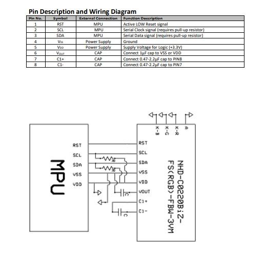
It's now nearly four years later and the datasheet, which has been revised 11 times since the original release, still remains confusing regarding the pinout. The page showing "Pin Description and Wiring Diagram" shows the pins in the reverse order than the previous page which is the "Recommended PCB Footprint". I bought two of these displays for evaluation and did not notice this problem until I ended up in the exact same situation as the original poster; according to the logic analyzer, both units communicate correctly over the I2C bus but neither displays anything. I'm now looking at ways around this problem by eliminating the display from the design.
0 -

Hi Dave,
We are sorry for the confusion regarding the pinout interpretation on this display. The wiring diagram on the schematic page is not intended to reflect the pinout locations on the LCD.
The mechanical drawings both on page 3 and on page 4 of the datasheet correctly identifies the LCD pin positions to be used for laying out the PCB.
Looking from the top (face) side of the display, pin 8 is correctly shown on the left side and pin 1 on the right side.
For the next revision of the datasheet, we will rotate the schematic image 90° to the right so that RST (pin 1) shows on top (as now shown in the attached image).
This will then match the Pin Description table where pin 1 is also on the top.
We hope this will eliminate any confusion regarding the pinout of this display.
Regards,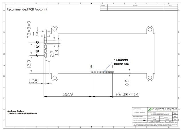
 0
0
Please sign in to leave a comment.
Comments
3 comments